LTC4350
4350fb
applicaTions inForMaTion
A timer is started as soon as the OV pin exceeds 1.220V .
The timer consists of a 6礎 current source into an external
capacitor on the TIMER pin. As soon as the voltage on the
TIMER pin exceeds 1.220V , the STATUS pin is pulled low.
There are two external power FETs in Figure 3. The FET
with its drain on the power supply side (left) and its source
on the load side (right) is used to block high voltage faults
from the load. If overvoltage protection is not needed, this
FET is omitted. Likewise, the FET with its drain on the load
side (right) can be eliminated if protection from a ground
short is not needed. The other use for the power FETs is
to allow hot swapping of the power supply. Hot swapping
will be discussed in a later section.
SOFT FAULTS
The existence of a share bus that forces tight regulation
of the system output voltage allows the system to detect
if the load current is not sharing properly. As mentioned
previously, the output of E/A2 will adjust until the measured
current equals the share bus value. If the power supply
output fails to share properly, the E/A2 output will hit the
plus or minus supply. The LTC4350 uses the over/under
current block to monitor the E/A2 output. This block
signals the logic that a soft fault has occurred if the E/A2
output goes out of the normal 0.5V to 1.5V range where
the I
OUT
block is active. After a timer cycle, the STATUS pin
indicates a soft fault. The timer consists of a 2礎 current
source into an external capacitor on the TIMER pin. As
soon as the voltage on the TIMER pin exceeds 1.220V , the
STATUS pin is pulled low.
The fault indication at the STATUS pin is disabled under
one condition. The E/A2 output can be less than 0.5V
when the load currents are low. In this case, it is desired
to disable the soft fault indication until the current is
higher. Higher current is defined as when the GAIN pin is
greater than 100mV .
The most common situations for soft faults are a discon-
nected power supply and the share bus shorts to V
CC
or
ground.
HOT SwAPPING
The LTC4350 controls external power FETs to allow power
supplies to be hot swapped in and out of the powered
system without disturbing the power buses. The gate of
the power FETs are slowly ramped up. This slowly charges
the power supply input and output capacitors, preventing
the large inrush currents associated with capacitors being
hot plugged into power buses.
When power is first applied to the V
CC
pin, the gate of
the power FET is pulled low. As soon as V
CC
rises above
the undervoltage lockout threshold, the chips UV pin is
functional. A 0.1礔 bypass capacitor is required on the V
CC
pin. If the V
CC
pin is tied to the same power supply output
that is being adjusted, then a 51?decoupling resistor is
needed to hold up the supply during a short to ground
on the supply output.
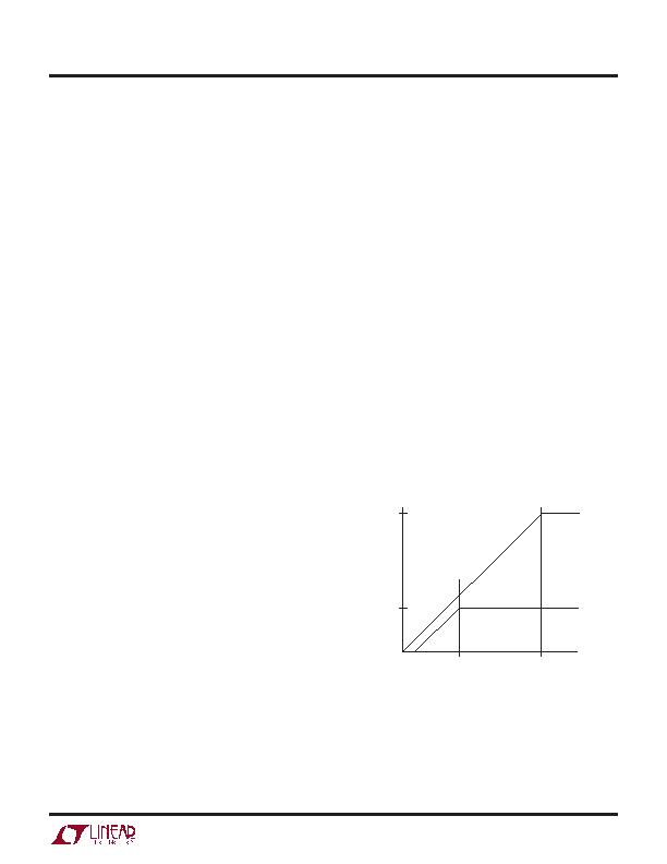
If the UV pin is greater than 1.244V , the gate of the external
FETs is charged with a 10礎 current source. The voltage at
the GATE pin begins to rise with a slope equal to 10礎/C
G
(Figure 4), where C
G
is the external capacitor connected
between the GATE pin and GND. This slow charging al-
lows the power supply output to begin load sharing in a
nondisruptive manner.
Figure 4. Supply Turn-On
CC
+ 10V
V
CC
4350 F04
t
1
t
2
GATE
V
OUT
SLOPE = 10礎/C
G
发布紧急采购,3分钟左右您将得到回复。
相关PDF资料
MAX1299CEAE+
IC TEMP SENS W/ADC 16-SSOP
MAX14544ETA+T
IC ACCY SWITCH OVP PROTECT 8TDFN
MAX1617AMEE+T
IC REMOTE/LOCAL TEMP SNSR 16QSOP
MAX1617MEE+T
IC REMOTE/LOCAL TEMP SNSR 16QSOP
MAX1619MEE+
IC TEMP SENSOR W/ALARM 16-QSOP
MAX1765EUE+
IC REG DL BST/LINEAR 16TSSOP
MAX1989MUE+
IC TEMP SENSOR REMOTE 16TSSOP
MAX31723MUA+
IC THERMOMETER/STAT SPI-3W 8UMAX
相关代理商/技术参数
LTC4350IGN#TR
功能描述:IC CNTRLR HOTSWAP LOADSHAR16SSOP RoHS:否 类别:集成电路 (IC) >> PMIC - 热交换 系列:- 产品培训模块:Lead (SnPb) Finish for COTS
Obsolescence Mitigation Program 标准包装:119 系列:- 类型:热交换控制器 应用:通用型,PCI Express? 内部开关:无 电流限制:- 电源电压:3.3V,12V 工作温度:-40°C ~ 85°C 安装类型:表面贴装 封装/外壳:80-TQFP 供应商设备封装:80-TQFP(12x12) 包装:托盘 产品目录页面:1423 (CN2011-ZH PDF)
LTC4350IGN#TRPBF
功能描述:IC CNTRLR HOTSWAP LOADSHAR16SSOP RoHS:是 类别:集成电路 (IC) >> PMIC - 热交换 系列:- 产品培训模块:Lead (SnPb) Finish for COTS
Obsolescence Mitigation Program 标准包装:119 系列:- 类型:热交换控制器 应用:通用型,PCI Express? 内部开关:无 电流限制:- 电源电压:3.3V,12V 工作温度:-40°C ~ 85°C 安装类型:表面贴装 封装/外壳:80-TQFP 供应商设备封装:80-TQFP(12x12) 包装:托盘 产品目录页面:1423 (CN2011-ZH PDF)
LTC4352CDD#PBF
功能描述:IC IDEAL DIODE CNTRL 12-DFN RoHS:是 类别:集成电路 (IC) >> PMIC - O 圈控制器 系列:- 标准包装:1,000 系列:- 应用:电池备份,工业/汽车,大电流开关 FET 型:- 输出数:5 内部开关:是 延迟时间 - 开启:100ns 延迟时间 - 关闭:- 电源电压:3 V ~ 5.5 V 电流 - 电源:250µA 工作温度:0°C ~ 70°C 安装类型:表面贴装 封装/外壳:16-SOIC(0.154",3.90mm 宽) 供应商设备封装:16-SOIC N 包装:带卷 (TR)
LTC4352CDD#TRPBF
功能描述:IC IDEAL DIODE CNTRL 12-DFN RoHS:是 类别:集成电路 (IC) >> PMIC - O 圈控制器 系列:- 标准包装:1,000 系列:- 应用:电池备份,工业/汽车,大电流开关 FET 型:- 输出数:5 内部开关:是 延迟时间 - 开启:100ns 延迟时间 - 关闭:- 电源电压:3 V ~ 5.5 V 电流 - 电源:250µA 工作温度:0°C ~ 70°C 安装类型:表面贴装 封装/外壳:16-SOIC(0.154",3.90mm 宽) 供应商设备封装:16-SOIC N 包装:带卷 (TR)
LTC4352CMS#PBF
功能描述:IC IDEAL DIODE CNTRL 12-MSOP RoHS:是 类别:集成电路 (IC) >> PMIC - O 圈控制器 系列:- 标准包装:1,000 系列:- 应用:电池备份,工业/汽车,大电流开关 FET 型:- 输出数:5 内部开关:是 延迟时间 - 开启:100ns 延迟时间 - 关闭:- 电源电压:3 V ~ 5.5 V 电流 - 电源:250µA 工作温度:0°C ~ 70°C 安装类型:表面贴装 封装/外壳:16-SOIC(0.154",3.90mm 宽) 供应商设备封装:16-SOIC N 包装:带卷 (TR)
LTC4352CMS#TRPBF
功能描述:IC IDEAL DIODE CNTRL 12-MSOP RoHS:是 类别:集成电路 (IC) >> PMIC - O 圈控制器 系列:- 标准包装:1,000 系列:- 应用:电池备份,工业/汽车,大电流开关 FET 型:- 输出数:5 内部开关:是 延迟时间 - 开启:100ns 延迟时间 - 关闭:- 电源电压:3 V ~ 5.5 V 电流 - 电源:250µA 工作温度:0°C ~ 70°C 安装类型:表面贴装 封装/外壳:16-SOIC(0.154",3.90mm 宽) 供应商设备封装:16-SOIC N 包装:带卷 (TR)
LTC4352HDD#PBF
功能描述:IC IDEAL DIODE CTLR W/MON 12-DFN RoHS:是 类别:集成电路 (IC) >> PMIC - O 圈控制器 系列:- 标准包装:1,000 系列:- 应用:电池备份,工业/汽车,大电流开关 FET 型:- 输出数:5 内部开关:是 延迟时间 - 开启:100ns 延迟时间 - 关闭:- 电源电压:3 V ~ 5.5 V 电流 - 电源:250µA 工作温度:0°C ~ 70°C 安装类型:表面贴装 封装/外壳:16-SOIC(0.154",3.90mm 宽) 供应商设备封装:16-SOIC N 包装:带卷 (TR)
LTC4352HDD#TRPBF
功能描述:IC IDEAL DIODE CTLR W/MON 12-DFN RoHS:是 类别:集成电路 (IC) >> PMIC - O 圈控制器 系列:- 标准包装:1,000 系列:- 应用:电池备份,工业/汽车,大电流开关 FET 型:- 输出数:5 内部开关:是 延迟时间 - 开启:100ns 延迟时间 - 关闭:- 电源电压:3 V ~ 5.5 V 电流 - 电源:250µA 工作温度:0°C ~ 70°C 安装类型:表面贴装 封装/外壳:16-SOIC(0.154",3.90mm 宽) 供应商设备封装:16-SOIC N 包装:带卷 (TR)